
Archivo:Opamptransistorlevelcolored.png
Opamptransistorlevelcolored.png (618 × 488 píxeles; tamaño de archivo: 10 kB; tipo MIME: image/png)
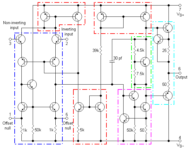
Transistor-level schematic for a 741 op-amp, color coded.
Resumen
(See w: Op-amp#Internal_circuitry_of_741_type_op-amp for the most recent description.)
From the diagram, the blue section is a differential amplifier. The base current of the inputs is not really zero, giving the 741 an input impedance of about 2 MΩ.
The sections in red are current mirrors. The input amplifier drives a current mirror load. The top left current mirror allows large common-mode voltages on the inputs without exceeding the active range of any transistor in the circuit. The top right current mirror provides a constant current load for the output circuitry, regardless of the output voltage . The lower current mirror has a very low collector current, because of the 5 kΩ resistor. It is used as a high-impedance connection to the negative power supply, to provide a reference without loading the input circuitry.
The offset null pins are used to remove any offset voltage that would exist at the output of the op-amp when zero signal is applied to the inputs.
The high voltage gain stage is NPN.
The green section is a voltage level shifter. It provides a constant voltage drop between the top and the bottom regardless of supply voltage. If the base current to the transistor is zero, and the voltage between base and emitter (and across the 7.5 kΩ resistor) is 0.625 V (a typical value for a BJT), then the current flowing through the 4.5 kΩ resistor will be the same, and will produce a voltage of 0.375 V. This keeps the voltage across the transistor, and the two resistors at 0.625 + 0.375 = 1 V. This serves as a bias for the two output transistors, to prevent crossover distortion. In some amps this function is achieved with diodes.
The capacitor is used as part of a low pass filter (on the base of an emitter follower) to reduce the frequency response of the amp to prevent oscillations. This technique is called Miller Compensation and functions as an internal capacitive feedback.
The output in cyan is a push-pull emitter follower amplifier. It is driven by a PNP emitter-follower. The output range of the amplifier is about 1 volt less than the supply voltage, since the collector-emitter voltage of the output transistors can never go completely to zero. The resistors in the output mean that the current provided by the output is limited (about 25 mA for the 741), and the output resistance is not zero without feedback. With negative feedback it approaches zero. The output stage has current limiting circuitry.
- Opis wyprowadzeń (cyfry oznaczają numery wyprowadzeń w standardowej obudowie ośmiokońcówkowej, końcówka nr 8 - nieużywana)
- Offset null - balans zera
- Inverting input - wejście odwracające
- Non-inverting input - wejście nieodwracające
- Vs- - minus zasilania
- Offset null - balans zera
- Output - wyjście
- Vs+ - plus zasilania
Op-amp transistor level
-
 Transistor level diagram of an op-amp
 -
 Sectioned transistor level diagram of an op-amp
 -
 Sectioned transistor level diagram of an op-amp with labeled transistors


Created by User:Omegatron using Klunky schematic editor, which the creator considers public domain (possibly with post-editing in the GIMP or Inkscape)
- Eres libre:
- de compartir – de copiar, distribuir y transmitir el trabajo
- de remezclar – de adaptar el trabajo
- Bajo las siguientes condiciones:
- atribución – Debes otorgar el crédito correspondiente, proporcionar un enlace a la licencia e indicar si realizaste algún cambio. Puedes hacerlo de cualquier manera razonable pero no de manera que sugiera que el licenciante te respalda a ti o al uso que hagas del trabajo.
- compartir igual – En caso de mezclar, transformar o modificar este trabajo, deberás distribuir el trabajo resultante bajo la misma licencia o una compatible como el original.

|
Se autoriza la copia, distribución y modificación de este documento bajo los términos de la licencia de documentación libre GNU, versión 1.2 o cualquier otra que posteriormente publique la Fundación para el Software Libre; sin secciones invariables, textos de portada, ni textos de contraportada. Se incluye una copia de la dicha licencia en la sección titulada Licencia de Documentación Libre GNU. |
(In short, this means that you can copy and modify the image freely as long as you provide attribution; preferably in the form of a link back to this page.)

|
File:OpAmpTransistorLevel Colored.svg es una versión vectorial de este archivo. Debería usarse esa versión en lugar de este archivo PNG.
File:Opamptransistorlevelcolored.png → File:OpAmpTransistorLevel Colored.svg
Para más información, lee Ayuda:SVG. |
 |
Historial del archivo
Haz clic sobre una fecha y hora para ver el archivo tal como apareció en ese momento.
| Fecha y hora | Miniatura | Dimensiones | Usuario | Comentario | |
|---|---|---|---|---|---|
| actual | 19:36 26 jun 2005 | | 618 × 488 (10 kB) | Omegatron | An electrical diagram created by User:Omegatron. (Uploaded with Wikimedia Commonplace.) Source: Created by User:Omegatron {{GFDL}}{{cc-by-sa-2.0}} Category:Electrical diagrams\ |
| 19:29 26 jun 2005 |  | 618 × 488 (10 kB) | Omegatron | An electrical diagram created by User:Omegatron. (Uploaded with Wikimedia Commonplace.) Source: Created by User:Omegatron {{GFDL}}{{cc-by-sa-2.0}} Category:Electrical diagrams\ | |
| 23:50 19 may 2005 |  | 618 × 488 (10 kB) | Julo | Operation amplifier 741 {{PD}} from en:wiki |
Usos del archivo
No hay páginas que enlacen a este archivo.
Uso global del archivo
Las wikis siguientes utilizan este archivo:
- Uso en en.wikipedia.org
- Uso en hr.wikipedia.org
- Uso en pl.wikipedia.org
- Uso en sl.wikipedia.org